

Smart Electronics 8 Layer Immersion Gold Impedance HDI Board
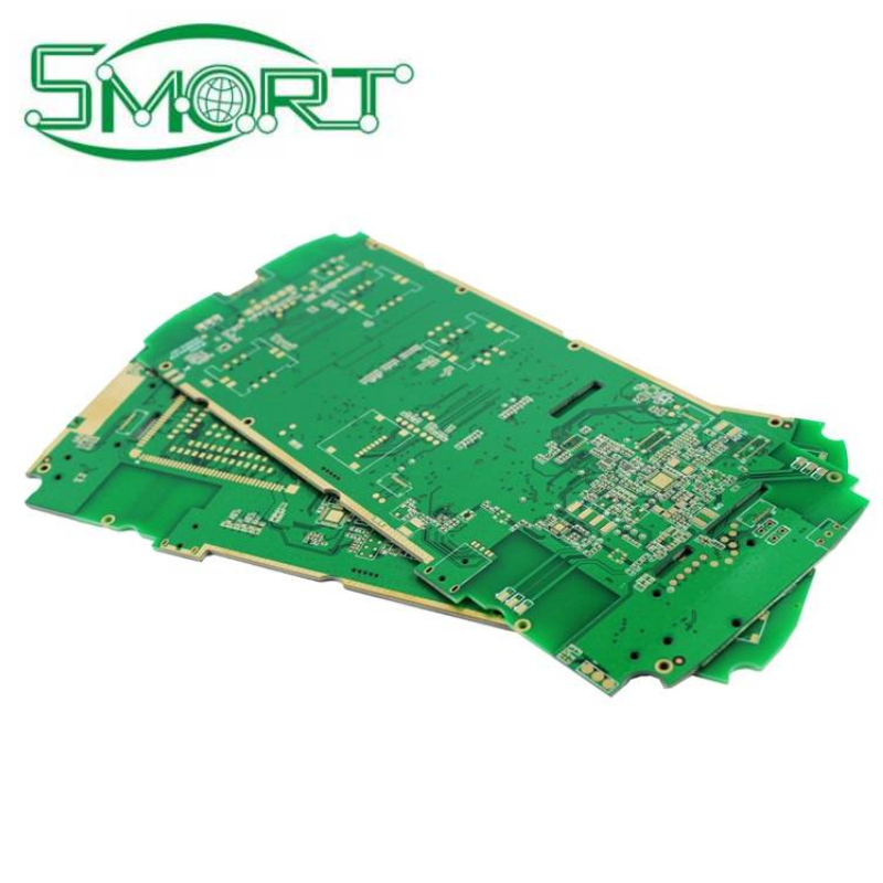
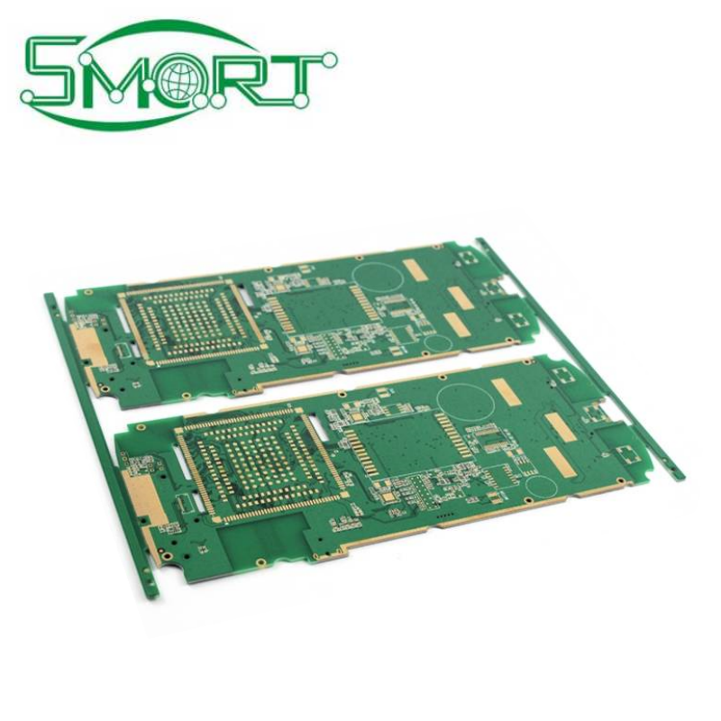
Smart Electronics 8 Layer Immersion Gold Impedance HDI Board
1.8-Layer Stack-up – Superior Signal & Power Integrity
2.HDI (Microvia) Technology – Maximizes Routing Density, Minimizes Size
3.Impedance Control ±10% – Ensures Stable High-Speed Signal Transmission
4.ENIG Surface Finish – Excellent Flatness, Solderability & Oxidation Resistance
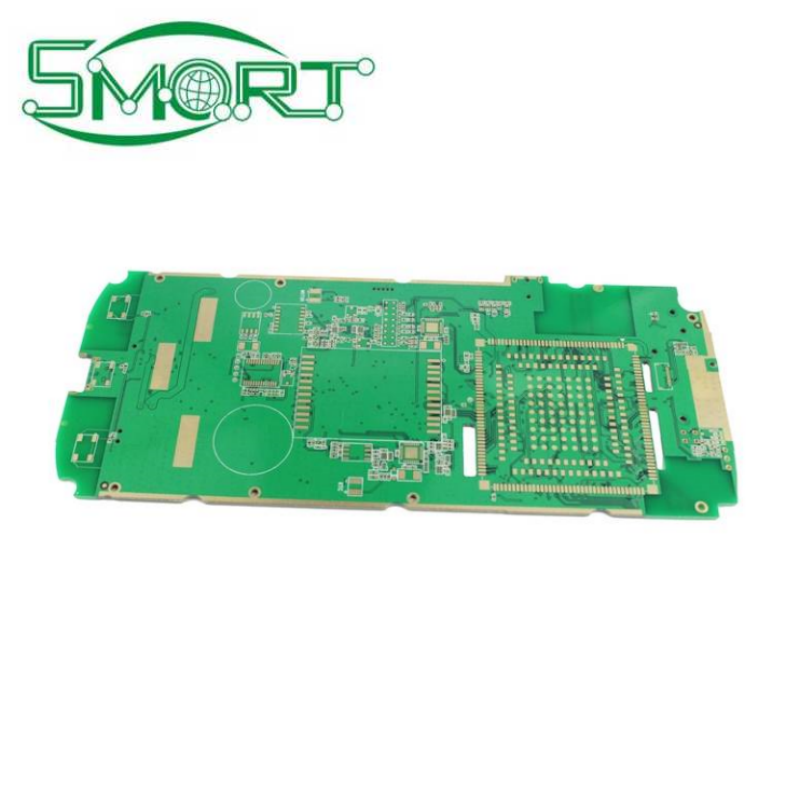
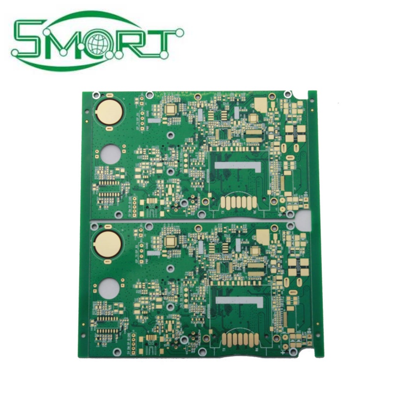
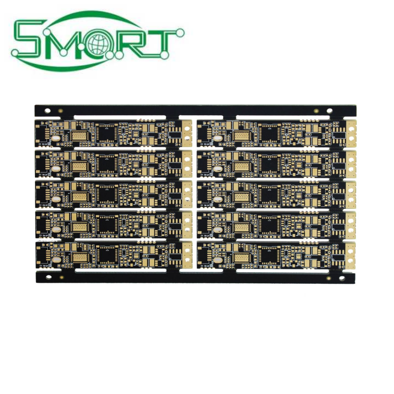
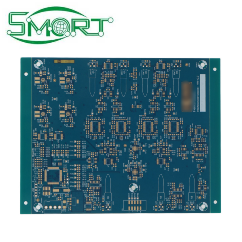
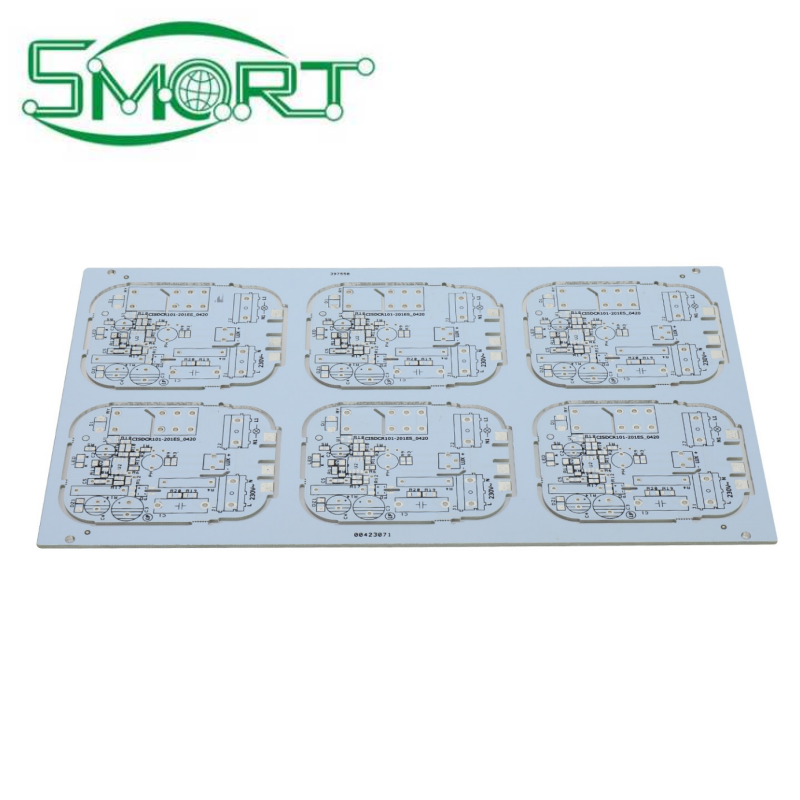
8 layer immersion gold impedance HDI board
Product Overview
Our 8-Layer ENIG Impedance Control HDI board is the cornerstone for core modules in modern, high-end electronic devices. Engineered to tackle design challenges of compact space, high signal speeds, and stringent reliability requirements, this product combines an 8-layer multilayer design, High-Density Interconnect (HDI) technology, precision impedance control, and Electroless Nickel Immersion Gold (ENIG) surface finish. It provides a stable and reliable platform for your communications equipment, industrial control systems, advanced computing, medical instruments, and aerospace applications.
Core Technologies & Advantages
1. 8-Layer Precision Stack-up
Superior Electrical Performance: The 8-layer structure provides ample ground and power planes, creating clear signal return paths. This effectively reduces electromagnetic interference (EMI) and power noise, ensuring stable circuit operation in complex environments.
Enhanced Routing Capability: Sufficient routing layers solve the interconnection challenges of high-density, multi-pin components (e.g., BGA, FPGA, high-speed processors), improving design success rates and flexibility.
2. HDI (High-Density Interconnect) Technology
Microvia (Blind/Buried) Design: Utilizes laser drilling to achieve direct and precise interconnections between layers, avoiding the space consumption of through-holes.
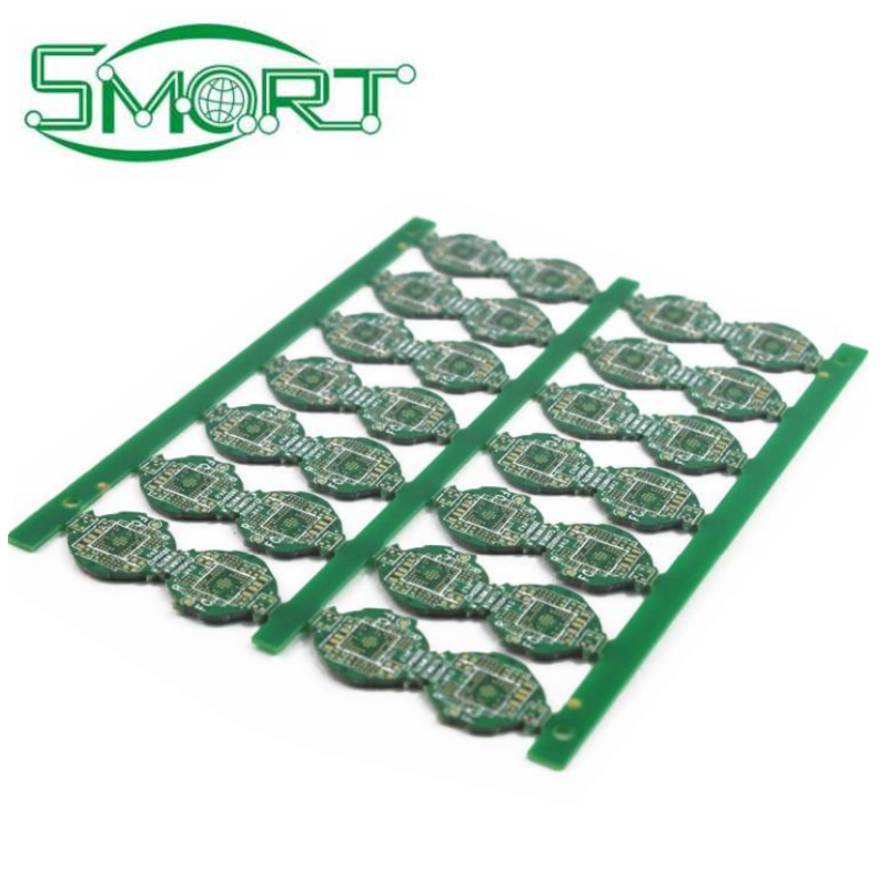
Optimal Space Utilization: Enables integration of more functionality into a smaller board area, a key technology for product miniaturization and thinning.
Improved Signal Quality: Shorter interconnect paths reduce signal delay and parasitic effects, particularly beneficial for RF and high-speed digital signals.
3. Precision Impedance Control (±10%)
What is Impedance Control? By precisely calculating and controlling trace width, thickness, dielectric thickness, and constant, the line impedance is matched to the driver's output and receiver's input impedance.
Core Value: Minimizes signal reflection and distortion during high-speed transmission, ensuring signal integrity and timing accuracy. This is critical for data rate and stability. We deliver high-precision impedance control within ±10% to meet stringent requirements for interfaces like PCIe, DDR4, and USB 3.0/3.1.
4. ENIG (Electroless Nickel Immersion Gold) Surface Finish
High Surface Flatness: The gold layer is extremely flat, ideal for soldering fine-pitch components (e.g., µBGA), preventing bridging or poor solder joints due to surface unevenness.
Excellent Solderability & Shelf Life: The gold layer prevents copper oxidation during storage, maintaining long-term solderability. The nickel layer acts as a barrier, preventing copper-gold diffusion and creating robust solder joints.
Reliable Contact Performance: Gold offers good conductivity and corrosion resistance, making it perfect for contact surfaces like gold fingers, test points, or switch contacts.
Typical Applications
Communications: 5G Base Stations/Terminals, High-End Routers, Network Switches, Optical Modules
Computing & Storage: Server Motherboards, AI Accelerator Cards, High-End GPUs, SSDs
Industrial & Medical: Industrial Control Boards, Advanced Test Equipment, Medical Imaging Devices
Automotive Electronics: ADAS/AD Control Units, Advanced Driver-Assistance Systems
Consumer Electronics: Flagship Smartphones, Drone Core Boards, Premium Wearables
Technical Specifications Table
| Parameter | Specification |
|---|---|
| Layers | 8 Layers |
| Base Material | FR-4 (High Tg), Mid-loss / Low-loss Materials Available |
| HDI Type | 1+N+1 (Blind & Buried Vias) or Higher Complexity Available |
| Min. Trace/Space | 3/3 mil (0.075/0.075 mm) or Finer |
| Min. Drilled Hole Size | Mechanical Drill: 0.2mm; Laser Drill: 0.1mm |
| Surface Finish | ENIG, Au Thickness: 0.05-0.1µm, Ni Thickness: 3-5µm |
| Impedance Control Tolerance | ±10% |
| Copper Weight | Inner Layer: 1oz (35µm), Outer Layer: 1oz (35µm) standard, Customizable |
| Solder Mask Color | Green, Black, Blue, White, etc. |
Why Choose Us?
Expert Support: Full-cycle technical support from stack-up design and impedance calculation to DFM analysis.
Stringent Quality Control: Adherence to IPC Class 2/3 standards, with Flying Probe Test, AOI Inspection, and impedance sampling to ensure specification compliance.
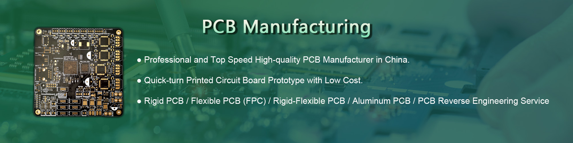
Rapid Response & Delivery: Advanced HDI production lines enable flexible and fast turnaround for prototypes and low-to-mid volume batches.
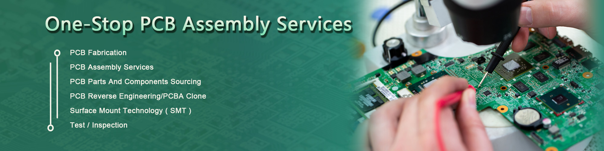
One-Stop Service: Complete electronic manufacturing services from PCB fabrication to component sourcing and PCBA assembly.


| SHENZHEN SMART ELECTRONICS CO.,LTD. |
|
|